


If you follow technology news often. You may have heard that Intel recently replaced its CEO.It's Pat Gelsinger, who started at Intel as a quality controller in 1979 before moving on to the 80386 processor development team and becoming the developer of the 80486 architecture (remember the Turbo button~). Pat was also named Intel's first Chief Technology Officer (CTO), and he founded the Intel Developer Forum (IDF), which strengthens the developer community for Intel architectures. The people who contributed to Intel's long dominance in the market As we can see for a while that How good is the technology of the chip? but no program used It's hard to sell anyway. and in the past He then moved to CEO at VMWare, a company specializing in The world's top virtualization platform before agreeing to return to help change the situation of Intel in the heat of competition with TSMC and AMD on February 15, 2021.
The first result is an announcement that will be open to the general public. As with the PS4/5 and XBOX One/X, the PS4/5 and XBOX One/X use specialized chips. It builds on the ground-breaking technology of AMD Ryzen and AMD RDNA , and announces that Intel will once again be a technology leader in 2025.
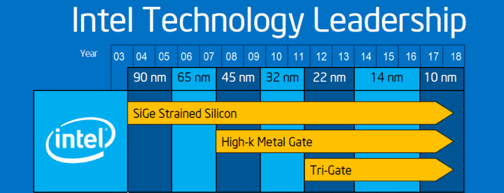
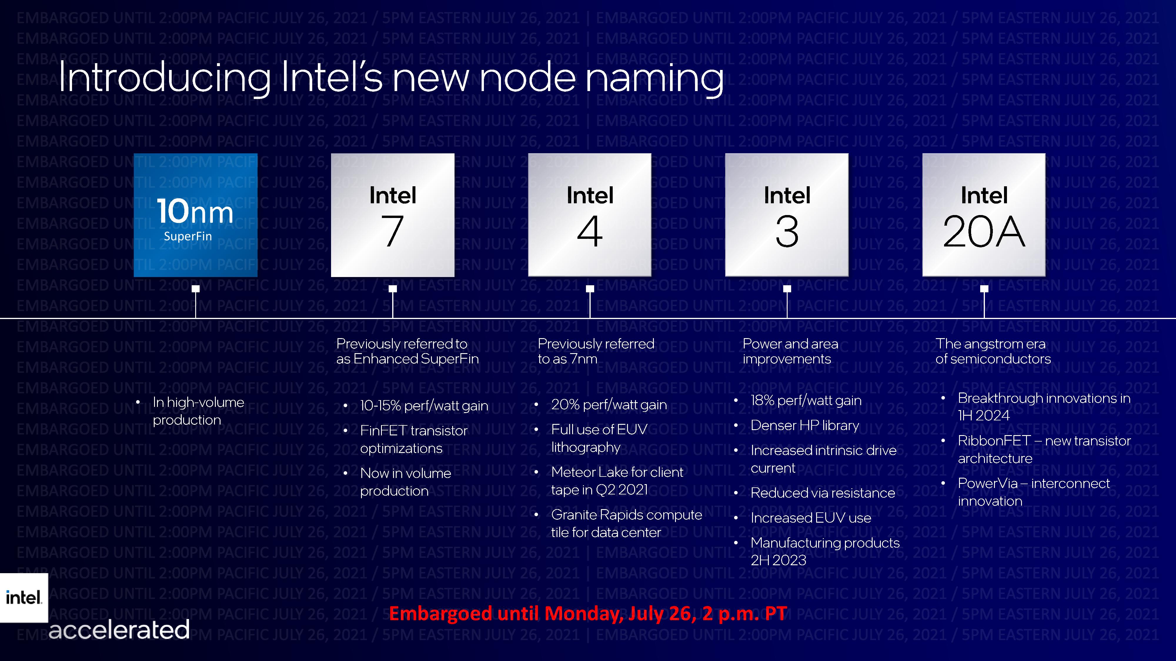
At Intel Accelerated on July 26, Pat outlined his plans for Intel to return to the top. By launching the Roadmap and changing the name of the new production technology.
By removing all nm~!
Why doesn't the nm number convey anything? And what exactly is it?
for that personally I have long felt that Intel made a serious mistake. that still refuses to change the name of the 14nm technology, but uses the ++++++ added at the end Maybe for the reason that Intel has announced a roadmap for a long time that it will be named 14, 10, 7 and fear that the name will change. It would be acceptable to accept the delay of 10nm technology (the size of the Transistor is not 10nm).
Before we get to the title Let's understand the origin of nm or Nano-meter a little bit first.
CPU fabrication involves projecting the image of a subject onto a piece of silicon wafer, which creates a CPU schematic. This manufacturing method is collectively known as Photolithography . By the way in depth how it can be done. Of course, it's his producer's secret.
The origin of this nm used to come from the size of a single transistor that could be projected onto a circuit. CPU circuits use billions of transistors connected to each other. Until it can process AND OR JUMP together until Windows let me type the block like now. and production development By figuring out a way to reduce the size of the transistor by one step, the manufacturer would call it "we developed a new process node".
The smaller the size of the transistor, the higher the density of the transistor, which has two broad effects:
- Use the same area but a more complex circuit This makes it possible to create a smarter CPU. in processing Makes the work efficiency higher, which means that in 1 Cycle can work more (Instruction per Cycle/Clock or IPC increases)
- It takes up less space with the original circuit. That is, the same circuit, as smart as before, the size is smaller, allowing us to have a high-performance CPU, but consume less power. emit less heat like now the mobile chip It can be called faster than computers 5-6 years ago.
However, since the introduction of FinFET technology since 2010 (though it was invented in the 1980s), the dimensions of the transistors, which were originally referenced to the dimensions of the Planar Transistors, no longer corresponded to the dimensions of the Transistors. Because FinFET transistors are 3D (non-planar) and have a much more complex structure.
Get to know FET and FinFET
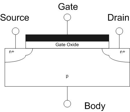
(image from Wikipedia)
For FET or Field-effect transistor , it is a type of Transistor that can control its resistance. By supplying power to the Gate pin to turn on or off the flow of electricity from the Source pin to the Drain (Channel) pin, which is the source of creating a MOSFET that is a Semiconductor. Necessary to create every electronic device in this world ever. If you look at the motherboard, the power supply unit (VRM) of the CPU also uses MOSFETs as a component in that circuit.
As for FinFET, it is a type of FET in which the gate is covered with a channel on all 3 sides so that the current that is supplied through the gate can create a nearly omnidirectional field effect instead of being able to create it from one side of the top. The video below, from 0:50 onwards, explains this visually.
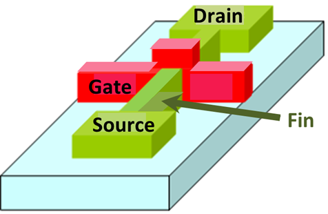
Image from Wikipedia
If you look at the illustration, you can see that 1 Transistor has components that are smaller than it. Especially the part that is the Fin that acts as a channel connecting the Source to the Drain, and it doesn't have a size of 22, 14, 10 or 7nm at all, which is why it's the reason why the nm numbers don't correspond to the 3D Transistor size. longer because its components are smaller. And it's also thick. If the transistor is 7nm wide but 10nm long and 14nm thick, how many nm should we call it? 😂
So why does Intel call it 10nm, but TSMC calls it 7nm (N7)?
From someone who has had a microscope, it was found that the size of the Intel 14nm++++++ and AMD 7nm (TSMC N7) Transistors are actually not twice as big as they should be. And as we said a moment ago, when a Transistor is 3 dimensions, which dimension will we take? Let's call it its size.
In fact, what Intel calls 22, 14, 10, 7 here comes from the fact that previously the Process Node was reduced in increments of about 30%, although the use of FinFET no longer reflects the size of the Transistor. (Since the Tri-Gate Transistor), but Intel still chooses to use nm numbers, reducing the number by 30% by approximately the same and seeing that 10nm was originally announced that it would It's been here since 2017.
For comparison on the Anandtech website , which I like to read a lot. have explored that OK, telling me this nm number, what is the density (Density) of the Transistor per 1 square millimeter area? Because this density is the most obvious measure. That can tell who's Process Node is more advanced and smaller than it really is. As previously mentioned, the higher the Density, the more intelligent we can produce chips. make it more efficient or it can make it use less power. But there is another note that each factory may use different methods of counting Transistors!
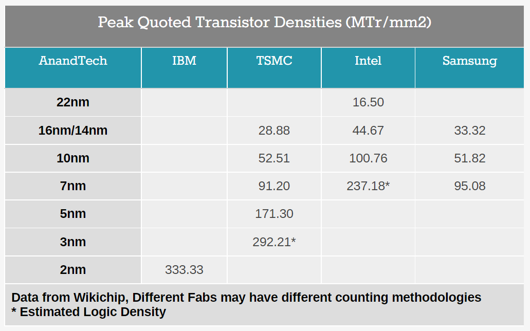
From the table (MTr/mm2 = Million Transistor per Square Millimeter or how many million transistors per 1 square millimeter area), it can be seen that the transistor density of the 14nm process node is 54% more than that of TSMC, which is called 10nm, and more than Samsung. 34% more, and if you look at the table, you will find that Intel 10nm Process Node has higher Transistor density than TSMC 7nm Process Node, which is why it is said that Intel 10nm is actually close. It's similar to TSMC 7nm or Samsung 7nm, and Intel claims that if people really care about it. He probably already knew it was just a name.
But it appears that the average customer is a media addict, anyway, 7nm is smaller than 14nm, do you understand!!!
Now it's too late to cheer for Intel to keep up....so it has to be called a new name!
Since TSMC has already begun producing chips in its TSMC 5nm Process Node, the Apple M1, A14 Bionic, Snapdragon 888/780G, Exynos 2100 and Kirin 9000 chips have twice the transistor density than Intel 10nm and Intel's 7nm plans. still far away is that it will start to produce It 's the second half of 2022. It makes Intel look very "lagging" right now because the name is still 1x behind, even if the Density is higher.
At Intel Accelerated, Intel announced its new manufacturing technology. Let it match all the villagers (Hmmm, just remembered?) because it's really taken in, no matter what factory. It uses machines from ASML to produce them as well, and every factory puts the money together ( Samsung invests in ASML following Intel and TSMC stakes ) is how good he or she is at customizing FET designs. However, there's no way to get a 30% difference in density!!!
In conclusion, therefore, it is the origin of the new name, which is precisely referred to by TSMC as follows.
(Photo courtesy of Anandtech)
Let's follow the schedule.
- Before: Intel 10nm SuperFin (10SF) is still called the same. Because already sold, it's the Tiger Lake chip (Intel Gen 11 H/U).
- The second half of 2021: from the original Intel 10nm Enhanced SuperFin (Oh, I thought Microsoft's Marketing to name it) changed to Intel 7 , that is, with a density of about 100M Transistor/mm2, the same as the current TSMC 7nm, after becoming The same is just the name change 🤣 By Alder Lake and Sapphire Rapids, which originally said it was 10nm, it would say Intel 7 instead
. As for TSMC, it is expected that the N4 that is an upgrade from N5 (in the original roadmap will be called N5P) will start within. It's already 2021, and it's expected that AMD Zen4 will use this N4 technology because desktop chips will be larger, harder to manufacture, and more costly. N5 must be solved for high yield first, then come to the audio production with larger chips. If TSMC is successful in starting production for AMD, it means that Intel will be following TSMC in terms of Transistor Density already this year.
- Within the second half of 2022: Originally called Intel 7nm, change to Intel 4. But now, if TSMC can follow the roadmap, it will be N3, which is expected to have a Density that is 23% higher than Intel 7nm (with TSMC saying that N3 will increase Density from N5 70%) If compared to the past, it is almost 1 Full Process Node apart, so it's not surprising that Intel calls it 4 instead of 3.
- Within the second half of 2023: from Intel 7nm+ to Intel 3 , this period will be equal to N3, but TSMC has not released a roadmap that is further than N3. Highlights of the TSMC Technology Symposium 2021... - SemiWiki
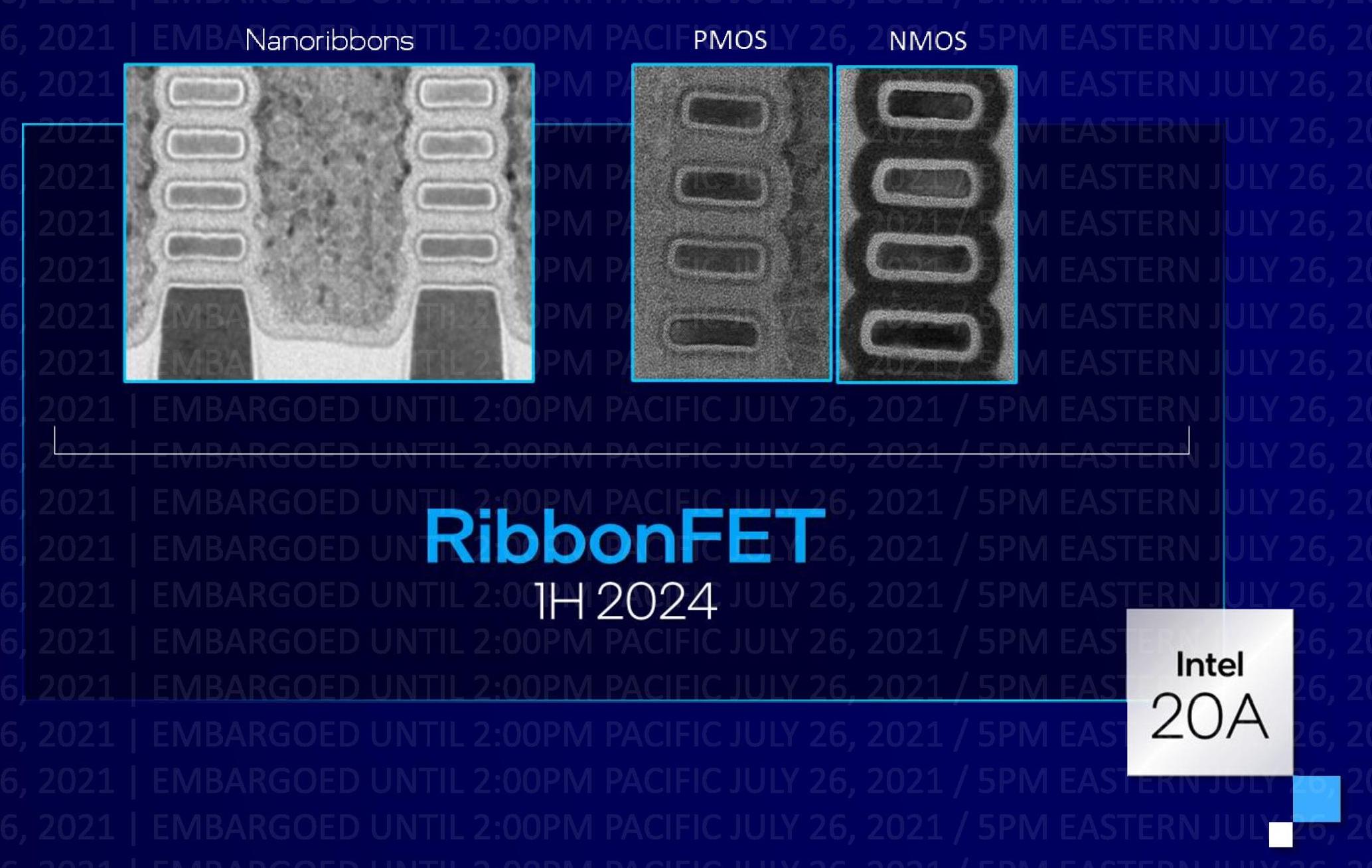
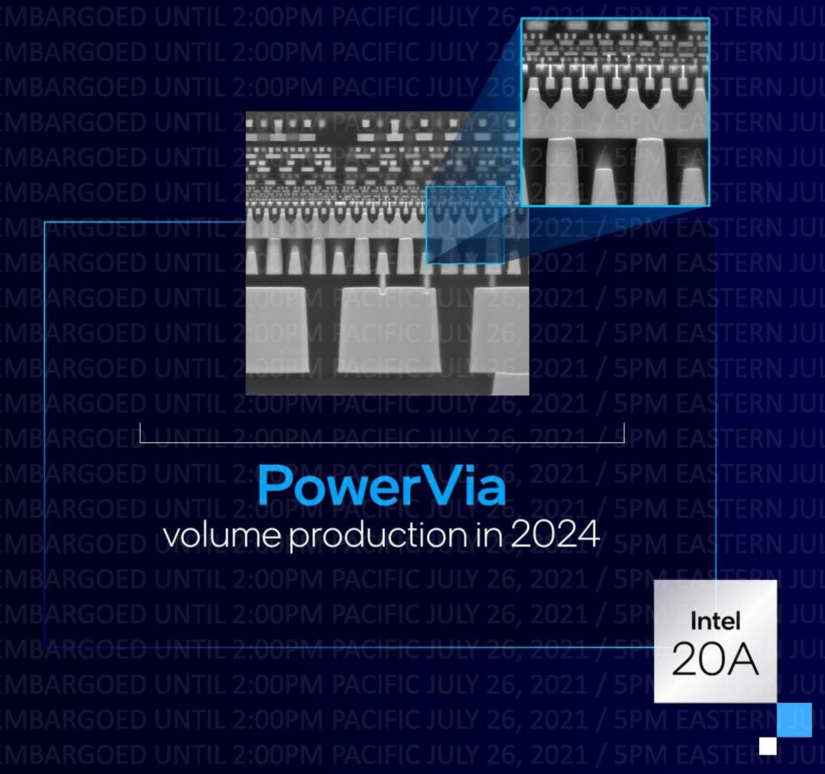
- 2024 - Intel 20A : is a new name , it will change the technology from using FinFET to RibbonFET that will be discussed later.
- 2025 - Intel 18A , which Intel expects to turn back into the market leader again in terms of Performance per Watt.
By the way, Intel is now a year behind TSMC, and Pat has a big job ahead of you to manage the development of the new Node as quickly as possible. to win the leadership of production technology back
But why is it called 20A???!!!? So what is A?
The Next Generation of Transistor and Angstrom Era
Once the nm is eliminated...Intel then introduced a new unit instead, it's A or Angstrom, but if you notice that Angstrom unit must be A type Å It's a smaller era of Transistors.
The Ångström unit defines 10Å as 1nm , and the average diameter of an atom is 0.3nm. If 20A (that's 2nm) is actually the size of a transistor, it's roughly the size of six atoms in a row. yes Probably not 🤣
IBM Research is the first technology center capable of producing chips. with technology at a level higher than TSMC's N3 (292MTr/mm2) at 333.33Mtr/mm2 Which is up 15%, so it deserves to be called 2nm (News: IBM Creates First 2nm Chip (anandtech.com) ) by Intel 20A will likely need to apply for some license patent from IBM to use with 20A of Certainly myself
For the new technology that will be used with 20A is GAA FET, also known as Gate-All-Around FET , it is another level of FinFET. The Gate is wrapped around the Channel, allowing it to control the conductivity from the Source to the Channel's drain. Getting around 4 directions from the first episode, only 3 sides in the case of FinFET/Trigate It is the last form of Multi-Gate Transistor that has been invented.
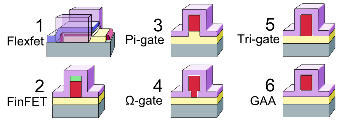
(image from Wikipedia)

The disadvantage of FinFet is that the size of the fin is limited to the ability to arrange the substance used to make the fin higher (in the picture, FinFET is 50nm), and if you look at the picture, you can see that the top fin is less thick than the sides. Bottom, we want to make the channel wider because the wider the channel (must pick up FinFET, it's up to see The height becomes the width) and a lot of current can pass through it. resistance is also lower The heat of the CPU comes from the resistance of the Transistor. Imagine that if we took a small wire, but connected to the Load that draws a lot of power, it will be hot. That 's it, and this CPU, it draws 100-200A of power ever.
Whereas GAA is horizontal which minimizes scaling constraints. But it must be nested in several layers. than to come out If anyone has ever used a 3D printer, they should be able to imagine that. Then we have to type the base as Gate, then type Channel, and then add the Gate material to it, alternating back and forth like this. to come out as GAAFET
by Intel called GAAFET that RibbonFET (PMOS and NMOS are a type of Transistor N and P) and choose to use Channel 4 stacked and said that just stacked 4 layers can provide current through the same FinFET with a smaller size. almost half Makes it possible to increase the Density of the Transistor again.
New Power Delivery Method Backside Power Delivery, PowerVia
Another issue that is a limitation in increasing the speed (GHz) of the CPU is the signal transmission within the chip itself.
Usually, the design of the chip is the design of the signal cable. (Interconnect) and wires (Power Delivery) mixed together under the Transistor for manufacturing reasons. which the power cable and the signal cable are close together It will interfere. The Power Delivery interferes with the signal of the Interconnect, causing the Bottleneck. The Interconnect will interfere with the Power Delivery, causing more resistance and heat up, causing the need to design a winding circuit to avoid each other, wasting space on the Wafer, which is expensive. Very expensive because the more space you can reduce, the more die can be produced per Wafer.
PowerVia technology is designed with the Transistor layer in the middle, the Interconnect layer on the top, and the Power Delivery layer on the bottom instead called Backside Power Delivery, and uses a new, smaller vias (connection pins) to connect the layers. Power Delivery with Transistor layer
wait and see
Although the name has been changed to be consistent with other competitors Intel is still a year behind TSMC in transistor density, if AMD Ryzen can start manufacturing with N4 technology. By 2021, by 2022, Intel will have to accelerate the development of Intel 4 in time to compete with the Zen 4 by Christmas 2022.
Hopefully then the covid will improve and ETH will change to Proof-of-Stake now, chips will be shortage again! 🤣